Multibit Electrically Reconfigurable Circularly Polarized Reflectarray Elements Based on Pancharatnam–Berry Phase Principle
IEEE AWPL, vol. 24, no. 12, pp. 4630–4634, Dec. 2025
你库里已经有一堆 1-bit 可重构反射阵:一个 PIN 二极管切两种状态,相位只有 0° 和 180° 两档。问题是档太少——相位量化误差大,旁瓣高、口径效率低。想加档,圆极化(CP)阵又很头疼:线极化可以靠变容管连续调谐,CP 的多比特电控一直没什么便宜好用的办法。
这篇的骚操作一句话:PB 相位
Pancharatnam–Berry 相位,几何相位的一种。圆极化波打到旋转 θ 角的各向异性单元上,反射波会白捡 2θ 的相位差——转多少得双倍,纯几何操作,不改变谐振
结果:2-bit 单元实测 11.1–12.5 GHz 插损 <1 dB、四档相位间隔约 90°;16×16 阵列 ±60° 扫描,口径效率 39.1%,比之前用 8 个二极管做 2-bit 的方案省一半管子。验证手段也有讲究:用波导模拟器(WGS)只做一个 2×2 小样就等效测了无限大阵。
1. 引言:1-bit 的天花板约 10 分钟
Abstract—P-i-n diode-based reconfigurable reflectarray antennas have gained attention for their flexible beam-steering, simplified design, and cost effectiveness. However, many existing designs offer only 1- or 2-bit phase reconfigurability, limiting radiation performance. In this letter, we present Ku-band reflectarray elements with both 2-bit and 3-bit electrical phase control for circular polarization. By leveraging the Pancharatnam–Berry phase principle, dynamic phase control is achieved through p-i-n diode switching. The proposed design is validated using a waveguide simulator (WGS), which confirms the 2-bit phase responses and shows excellent agreement with full-wave simulations. Measured results demonstrate 2-bit phase quantization over an 11.1 GHz to 12.5 GHz range (11.9% bandwidth) with insertion losses below 1.0 dB and cross-polarization levels under −15 dB. Furthermore, simulated performance of the 3-bit element reveals consistent 45° phase intervals. To verify array-level performance, 16 × 16 RRAs based on both 2-bit and 3-bit elements are implemented. This multibit reconfigurable strategy enhances reflectarray performance and offers increased design versatility for advanced Ku-band applications.
Reconfigurable reflectarray (RRA) antennas with dynamic beam control have garnered significant attention for applications in wireless communications and sensing systems [1]. These antennas enable versatile manipulation of electromagnetic waves, supporting beam steering, information sensing, and imaging functionalities. In contrast to conventional phased arrays [2], [3], [4], which require bulky feeding networks and expensive transceiver modules, 1-bit RRAs employing spatial feeding techniques offer a cost-effective solution for wide-angle beam scanning [5], [6], [7]. RRAs are typically implemented using various tuning elements, including p-i-n diodes, varactors, radio-frequency microelectromechanical systems (RF-MEMS), graphene, and liquid crystals [1]. Among these, PIN diode-based 1-bit RRAs have attracted considerable interest due to their affordability, simplicity, and widespread availability [8]–[12]. As demonstrated in [9], altering the state of a p-i-n diode enables tuning of the resonant frequency and induces phase reversal, thereby achieving 1-bit phase adjustment for linearly polarized (LP) operation.
Researchers have further explored 1-bit circularly polarized (CP) RRAs based on p-i-n diodes [13], [14], [15] and by employing an element rotation method [16], which utilizes physical or mechanical rotation for phase tuning. However, 1-bit designs inherently suffer from phase quantization errors, resulting in reduced aperture efficiency and elevated sidelobe levels (SLLs). To mitigate these limitations, multibit phase control is essential. Existing approaches for multi-bit or continuous CP phase tuning include mechanical methods [17], [18], [19] and varactor-based designs [20]. In comparison, p-i-n diodes present a cost-effective alternative characterized by lower insertion losses and simpler biasing requirements, rendering them highly suitable for multibit CP RRAs.
To date, only one study has demonstrated a p-i-n diode-based wideband 2-bit CP RRA with ±60° scanning and improved efficiency [21]. A similar principle has been applied using MEMS technology for 2-bit LP reconfigurability; however, this approach introduces additional complexity [22]. In this work, we present a Ku-band 2-/3-bit electrically controlled CP RRA element based on an innovative design approach that is scalable to multibit phase control. The key innovation involves the integration of multiple p-i-n diodes around the reflective patch, enabling simulation of physical rotation via controlled diode switching to achieve the desired phase response.
This letter also presents the use of the waveguide simulator (WGS) method for CP element testing. Section II details the design and operating mechanism. Section III outlines the measurement setups and experimental results, and Section IV concludes the letter.
- phase quantization error
- 相位量化误差。阵面需要的补偿相位是连续的,但只有 2^n 档可用,硬凑出来的误差。1-bit 时最大误差 ±90°,是旁瓣和效率损失的元凶。
- aperture efficiency
- 口径效率。实际增益相对理想均匀口径增益的比值,反射阵的终极成绩单一。这篇做到 39.1%。
- SLL (sidelobe level)
- 旁瓣电平。主瓣之外最大副瓣的相对强度,量化误差的直接受害者。
- spatial feeding
- 空间馈电。馈源在远处直接照射阵面,不需要功分网络,反射阵便宜的根本原因。
2. PB 相位:转一倍,得两倍约 6 分钟
The proposed RRA element adopts the Pancharatnam–Berry (PB) phase principle [23], [24], [25], where the CP reflection phase equals twice the element's rotation angle. For clarity, we briefly introduce the PB principle used here. As shown in Fig. 1(a), under left-hand circular polarization (LHCP) excitation along the -direction, the incident electric fields () is written as
Here, denotes the vector electric of the incident wave, is the free-space wave number, is the angular frequency.
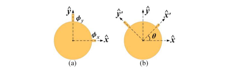
According to the basic rotational transformation matrix [24], when the element is rotated counterclockwise by an angle [Fig. 1(b)], the corresponding rotation matrix is . Then, the reflected wave can be written as
where and represents the reflection phases for x- and y-polar components. If , we have
This represents an LHCP reflected wave with a phase shift of , showing the CP reflection phase varies twice the cell's rotation angle. Conversely, under right-hand circularly polarized (RHCP) excitation, the phase shifts as .
- LHCP / RHCP
- 左/右旋圆极化。电场矢量旋转方向相反的两种圆极化,互为交叉极化。
- rotation matrix
- 旋转矩阵。描述坐标系(或结构)转 θ 角后矢量分量怎么变的 2×2 矩阵,PB 推导的全部'机关'。
3. 2-bit 单元:四根延时线伪造旋转约 12 分钟
As shown in Fig. 2, the proposed 2-bit CP RRA element uses a dual-layer substrate without air gap, comprising a reflective patch and bias circuit separated by a ground plane. The upper substrate is Arlon AD255 (εr = 2.55, tanθ = 0.0014, h1 = 1.5 mm), and the lower is FR-4 (εr = 4.4, tanθ = 0.02, h3 = 0.5 mm), bonded with an FR-4 adhesive film (h2 = 0.1 mm). A regular octagonal patch on the upper layer connects to ground via a blind via, acting as the main scatterer for CP phase control. Four identical phase delay lines at 45° intervals integrate p-i-n diodes (P#1–P#4) to dynamically adjust current paths and electrical lengths for precise phase tuning.
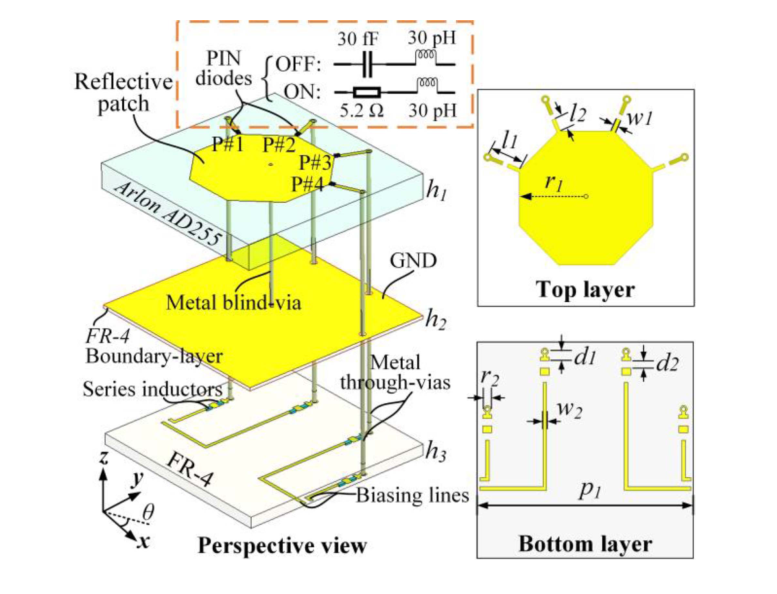
The DC bias circuit on the lower layer connects to delay lines through metallic vias. We employed the flip-chip MACOM MADP-000907-14020 PIN diode, modeled as an equivalent series circuit in simulations (Fig. 2). To save space, traditional quarter-wavelength radial stubs for RF signal choking were replaced by inductors. Each bias line includes two muRata LQW15AN3N2C00D (3.2 nH, SRF = 14 GHz) inductors, providing 6.4 nH for RF suppression.
Fig. 3(a) presents the simulated element response under two orthogonal incident waves, x′- and y′-polarizations, with P#2 "ON" and all other diodes "OFF," showing that the y′-polarized component follows an extended current path. The green dashed line indicates a roughly constant phase difference of 180° ± 10° between x′- and y′-components across 11.15 GHz to 12.2 GHz. Within this range, Sx′x′ and Sy′y′ magnitudes remain above −1 dB and approximately balanced, enabling the generation of a CP reflected wave with an axial ratio (AR) below 3 dB.
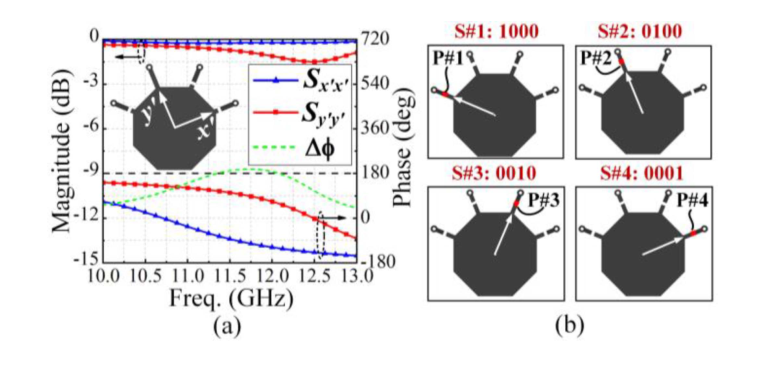
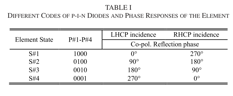
To achieve 2-bit phase quantization with uniform 90° steps, the element emulates four rotational states at 45° intervals by electronically controlling integrated p-i-n diodes, while retaining a fixed physical structure. In operation, one diode is ON and the others are OFF, forming an asymmetric current path on the otherwise symmetric element. As shown in Fig. 3(b), selective diode switching effectively emulates physical rotation, enabling discrete 2-bit reflection phase control. With ON/OFF represented as binary 1/0, phase states are encoded using 4-bit control logic (Table I). Under LHCP illumination, the element provides four reflection phases (0, π/2, π, 3π/2), corresponding to 2-bit quantization. These states, S#1–S#4, represent virtual rotations defined in the idealized configuration of Fig. 2(b).
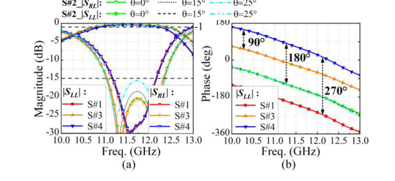
Simulation results were obtained in Ansys HFSS using Floquet excitation and primary–secondary boundaries. Fig. 4 shows the performance of four states under LHCP illumination. Owing to symmetry, states S#1 and S#4 exhibit similar amplitudes, as do S#2 and S#3. Fig. 4(a) shows copolarized (SLL) magnitudes above −1 dB and cross polarized (SRL) below −15 dB, yielding an AR under 3 dB from 11.17 GHz to 12.15 GHz. Fig. 4(b) confirms ∼90° phase differences among the four states across the band, verifying effective 2-bit CP phase quantization. Additionally, the response of state S#2 under oblique LHCP incidence shows stable copolarized magnitude and phase, with cross-polarized components below −15 dB up to 25°, demonstrating excellent angular stability. These results confirm the element's reliable 2-bit phase quantization under CP excitation, making it highly suitable for electronically scanned reflectarray applications.
- phase delay line
- 相位延时线。一段蛇形微带线,接通后给电流加额外电长度,这里是'伪造旋转'的执行机构。
- one-hot 控制
- 任一时刻只有一个二极管导通的编码方式(1000/0100/…)。控制简单,但 n 档要 n 个管子。
- axial ratio (AR)
- 轴比。CP 纯度的度量,<3 dB 视为合格圆极化。两个正交分量幅度相等、相位差 90° 时 AR 最优。
- Floquet 边界
- 周期边界条件,仿一个单元等效无限大阵。反射阵单元仿真的标配。
4. 3-bit 扩展与波导模拟器实测约 12 分钟
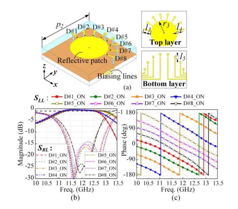
Building on the PB phase principle and the 2-bit implementation in Section II-A, a 3-bit CP RRA element is developed by adding four more phase delay lines, each integrated with a PIN diode, as shown in Fig. 5. The design features a circular reflective patch and eight identical delay lines with PIN switches (D#1–D#8). According to the PB principle, this design yields a theoretical 22.5° phase interval between adjacent lines. Similar to the 2-bit case, reflection phase control is achieved by switching the diodes. Fig. 5(b) and (c) shows the simulated coefficients and phases under LHCP incidence. From 11.3 GHz to 12.52 GHz, adjacent states exhibit ∼45° phase spacing, with copolarized magnitudes exceeding −1 dB and cross-polarized levels maintained below −15 dB.
Recent studies have validated the reliability of WGS for element testing [9], [12], [26], but CP reflectarray characterization in waveguides remains limited. Here, we adopt an orthomode transducer (OMT)—previously used for cross polarization and transmissive CP wave tests [9], [26]—to separate orthogonal linear polarizations.
To validate the proposed RRA element, a 2 × 2 array was fabricated [see Fig. 6(a)], enclosed by ground planes and periodic metallic vias to suppress substrate modes. As shown in Fig. 6(b), the test setup includes the device under test (DUT), a waveguide transition, two coax-to-WR75 adapters, and the OMT. Operating from 10.6 GHz to 12.8 GHz, the OMT offers 30 dB isolation and features an 18 mm test port, while the prototype measures 24 mm × 24 mm. An ad-hoc waveguide transition with a length of 20 mm (0.76λ0) and a tapered circular-to-square cross section was designed to ensure impedance matching. Bias voltages were set to ±3.3 V for forward and reverse operation.
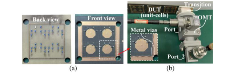
Calibration of the waveguide transition and OMT was performed via the short-circuit line method. After calibration, the elements (DUT) were placed at the test port. Full characterization involved measuring the S-parameters (), including magnitudes and phases (), with port definitions shown in Fig. 6(b). As both ports are linearly polarized, the orthogonal components were combined with a ±90° phase shift to derive the CP reflection coefficients, as defined in [26]:
where R represents the RHCP component and L signifies the LHCP component.
- waveguide simulator (WGS)
- 波导模拟器。利用波导壁边界等效无限周期阵环境,用几个单元的小样完成单元级实测,省掉加工整阵的成本。
- orthomode transducer (OMT)
- 正交模变换器。把波导里两个正交线极化模式分离到两个端口的器件,这里是 LP→CP 测量的桥梁。
- substrate mode
- 介质板表面波模式。能量沿介质板横向泄漏,小样边缘尤其严重,用过孔围栏抑制。
- short-circuit line calibration
- 短路传输线校准法。用已知短路/传输标准件把系统误差从参考面移除。
5. 成绩验收:单元、阵列与同行对比约 12 分钟
Fig. 7 compares simulated and measured results under CP incidence. In Fig. 7(a), the minimum measured insertion losses for states S#1–S#4 are 0.62 dB, 0.42 dB, 0.43 dB, and 0.65 dB, closely matching simulated values of 0.38 dB, 0.33 dB, 0.36 dB, and 0.42 dB. Across 11.1 GHz to 12.5 GHz (11.9% bandwidth), measured losses stay below 1 dB, with simulations showing similar performance over 10.8 GHz to 12.25 GHz. Additionally, the measured cross-polarized components for all states remain below −15 dB (AR < 3 dB) over the frequency range of interest.
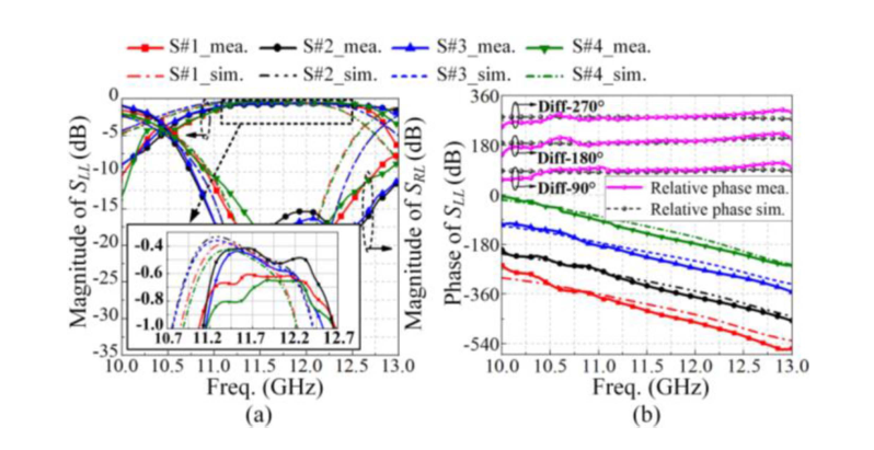
Fig. 7(b) shows strong agreement between measured and simulated reflection phases. The phase differences between adjacent states remain near 90° across the band: S#1–S#2, 83°–99°; S#1–S#3, 185°–210°; and S#1–S#4, 275°–295°. These phase differences align well with simulation, confirming the element's 2-bit phase reconfigurability under CP excitation.
The measured magnitude responses exhibit a slight shift toward higher frequencies compared to simulations. This discrepancy is attributed to the integration of an ad-hoc waveguide transition, calibration errors, manufacturing tolerances, and assembly misalignment. Nonetheless, the WGS method accurately captures the CP RRA element's phase states, thereby validating the method's overall accuracy in reproducing the intended phase characteristics.
To further validate the feasibility of the proposed RRA element, 2-bit and 3-bit CP 16 × 16 RRAs (7.4λ0 × 7.4λ0) were designed and illuminated by an LHCP horn (−20° offset, F/D = 1.23), as shown in Fig. 8(a). The phase compensation diagrams for different beam directions are shown in Fig. 8(b).
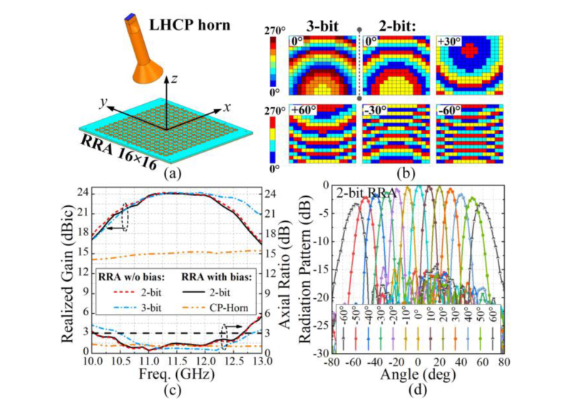
Fig. 8(c) presents the simulated broadside gains and ARs of both RRAs, with key metrics summarized in Table II. The AR < 3dB bandwidth range from 10.1 GHz to 12.6 GHz (22%) and 10.5 GHz to 12.8 GHz (19.7%) for the 2-bit and 3-bit CP RRAs, respectively. Furthermore, the performance of the 2-bit RRA integrated with the complete bias network is evaluated, indicating minimal impact and validating the effectiveness of the bias network design. Therefore, the trade-off—greater design complexity in exchange for enhanced multibit phase tunability—is considered acceptable. Fig. 8(d) demonstrates 2-D beam scanning at 11.6 GHz, achieving ±60° steering with a scanning loss below 3.35 dB and a sidelobe level under −15.5 dB at broadside direction. Due to the inherent symmetry of the proposed element, RHCP performance can be obtained by replacing the LHCP horn without altering the RRA.
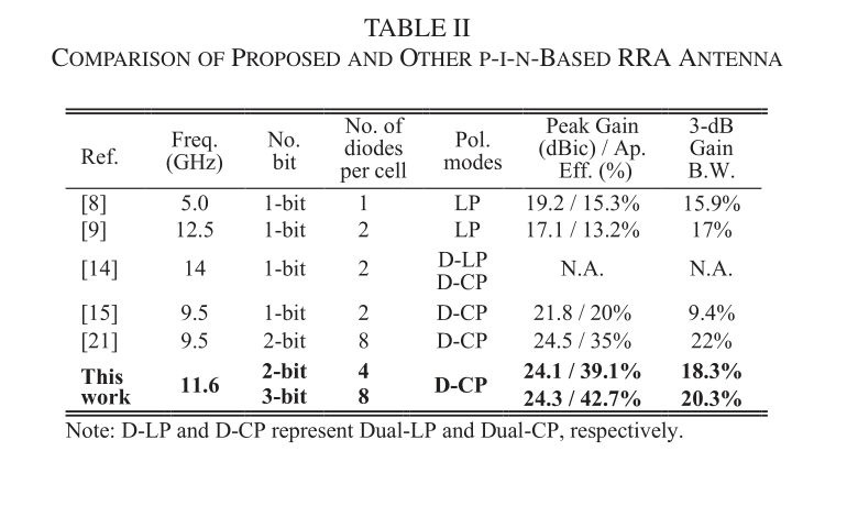
Table II compares the proposed p-i-n diode-based RRA with related works. Compared with the design in [21], which uses eight PIN diodes, the proposed element achieves stable 2-bit phase quantization with only four diodes, thereby reducing complexity and cost. The peak gain of the 2-bit CP RRA reaches 24.1 dBic at 11.3 GHz, with an aperture efficiency of 39.1%. Moreover, by increasing the number of p-i-n diodes per element to eight based on the same design concept, 3-bit phase quantization is realized. This novel design approach can be easily extended to arbitrary-bit element configurations, enabling flexible and scalable phase control.
In this letter, we propose a novel method for designing arbitrary-bit phase RRA elements. As a proof of concept, a 2-bit element is first designed and validated using a 2 × 2 prototype. The measurements based on the WGS method closely match the simulation predictions. A stable 2-bit phase quantization is achieved over the 11.1 GHz to 12.5 GHz band, with insertion losses below 1 dB. Furthermore, by extending the same design principle and implementation mechanism, a 3-bit element is also developed, exhibiting clear 45° phase steps in simulation. To verify array-level performance, 16 × 16 RRAs are implemented for both 2-bit and 3-bit cases. The results demonstrate wide AR bandwidths, ±60° beam scanning, and high aperture efficiency. These results validate the scalability of the proposed approach to arbitrary-bit electrically reconfigurable CP elements. With robust performance and wide bandwidth, the design strategy shows strong potential for advanced space and satellite communication applications.
- insertion loss
- 插入损耗。反射时白白损失的能量,直接吃掉增益。本文 <1 dB 属于优秀。
- scanning loss
- 扫描损耗。波束扫离法向时增益的下降,±60° 处 <3.35 dB。
- F/D
- 焦径比。馈源焦距与阵面口径之比,决定照射锥削,1.23 属常见取值。
- dBic
- 相对理想圆极化各向同性辐射器的增益单位,CP 天线专用。
- 回到 Obsidian,打开 [[P18-Multibit Electrically Reconfigurable Circularly Polarized Reflectarray Elements Based on Pancharatnam-Berry Phase Principle]],用你自己的话写下:
- 1. 『对称结构 + 不对称偏置 = 虚拟旋转』这个思想,和你库里哪篇论文的设计可以类比?(提示:P05 的旋转是真转)
- 2. PB 相位的前提条件是什么?这篇是怎么在 Fig. 3(a) 里验收它的?
- 3. WGS 测 CP 的整条链路(小样 → OMT → 公式(4) 合成)你能复述出来吗?
- 写完三条,这篇才算真正读完。