A Broadband Dual-Polarized ME-Dipole Antenna Array for Millimeter-Wave Applications
IEEE AWPL, vol. 23, no. 11, pp. 3456–3460, Nov. 2024
毫米波双极化阵一直在三件事里打架:带宽、层数、两路极化长得像不像。贴片/缝隙简单但只有约 10% 带宽;SIW 馈电能到 20%,但层数和剖面往上堆;交叉 L 探针可以把带宽拉过 40%,代价是多层、贵、难做进手机。
这篇的骚操作一句话:把 Luk 那套金属块 ME 偶极子
magneto-electric dipole,电偶极子 + 磁偶极子互补,E/H 面方向图接近,带宽宽、方向图稳。祖师是库里的 [[P10]]SIB
substrate integrated block,基板集成块。四根接地柱把方形贴片撑成一块"砖",电流路径还在,但砖与砖之间腾出了给正交探针交错的空间
结果:3×3 实物交叠阻抗带宽 36.2%(21.3–30.7 GHz,盖住 5G FR2 的 n257/n258/n261),峰值增益 14.7 dBi,带内起伏 2 dB,口径效率 67.5%。辐射一层、馈电一层。通讯作者 Fan Wu,东南大学毫米波实验室。
1. 引言:带宽、层数、极化,三选二约 10 分钟
Abstract—A magneto-electric dipole implemented using substrate integrated blocks (SIBs) is proposed for broadband dual-polarized array application. Facilitated by the SIB-based design approach, an interlaced arrangement of the perpendicular feeding probes is developed for dual-polarization excitation. While maintaining the wideband feature and single-layered antenna structure, nearly identical radiation characteristics for the two polarizations have been achieved. Additionally, the enlarged probe-to-probe distance increases the degree of design freedom for the feeding network. As a proof-of-concept, a 3 × 3 single-layered antenna array fed by a single-layered dual-polarization microstrip-line feeding network is designed and fabricated at the 5G millimeter-wave frequency band. The measured results indicate that the array prototype has a wide overlapped impedance bandwidth of 36.2%, covering from 21.3 to 30.7 GHz, within which a maximum gain of 14.7 dBi and a gain variation of 2 dB are maintained. The broadband performance, single-layered radiating structure, and nearly identical performance of two polarizations make the proposed design attractive for applications including 5G and beyond.
The increasing demand for wireless communication systems characterizing low latency and high system capacity has propelled the elevation of communication frequency, especially the exploration of 5G millimeter-wave (mmW) bands. Several 5G frequency range 2 (FR2) operating bands have already been standardized [1]. Therefore, research on broadband mmW antenna arrays holds significant importance in achieving high system capacity and addressing the increased path loss associated with 5G mmW high-frequency transmission. Particularly, considering the integration requirements with 5G devices, a pressing demand arises for wideband mmW antenna arrays with the advantages of simple structure, low cost, and stable radiation performance [2]. Simultaneously, the dual-polarization characteristic is required to mitigate the multipath fading effects at high frequencies and minimize polarization mismatch.
Over the past decade, sustained research has been conducted on the development of mmW dual-polarized antenna arrays. Slot and patch antennas have undergone substantial developments at mmW dual-polarized antennas [3], [4], [5], [6]. These designs, while simple in structure, can only achieve narrow impedance bandwidths of around 10%. Afterward, by adopting feeding techniques based on substrate-integrated waveguide (SIW) structure, cross-slot coupling, or orthogonal aperture-coupled stripline, the operating bandwidth of mmW dual-polarized antenna arrays has been extended to about 20% [7], [8], [9]. However, the structures of these antenna arrays are relatively complex, featuring a comparatively high profile or an excessive number of substrate layers, which are not feasible for deployment in portable 5G devices.
Magneto-electric (ME) dipole antennas, with a wide impedance bandwidth and stable radiation performance, are competitive solutions to achieve mmW antenna arrays [10], [11], [12], [13], [14], [15], [16], [17], [18], [19]. By using SIW feeding structures, mmW dual-polarized ME-dipole antenna arrays have been realized in [11] and [12]. Unfortunately, in these SIW-fed antennas, the bandwidth limitation of the SIW-feeding structure curtails the further expansion of the achievable bandwidth of the antenna. Subsequently, by utilizing crossed L-shaped probes, wideband dual-polarized ME-dipole antenna arrays, which achieve impedance bandwidths of over 40%, are reported in [13], and [14]. However, the implementation of such dual-polarization feeds and power-dividing networks requires a rather complex multi-layer structure that increases the fabrication cost.
In this letter, based on the ME dipole implemented using metallic blocks in [20], a block-shaped structure named substrate integrated block (SIB) is proposed. The SIB is a substrate-integrated form of the metallic blocks. By introducing the SIB, a broadband dual-polarized ME-dipole antenna array is presented. The dual-polarized radiation is excited by using two groups of interlaced perpendicular L-shaped feeding probes. As such, balanced radiation performances for the two polarizations can be achieved, and both the antenna structure and feeding networks can be implemented on a single layer. Compared to previously reported work, this design requires only two substrate layers, providing notable advantages of simple structure and low cost. The measured results of the proposed array show a wide overlapped impedance bandwidth of 36.2%, as well as a stable gain in the operational frequency range, which covers the 5G FR2 bands n257, n258, and n261.
- SIB (substrate integrated block)
- 基板集成块。把金属块 ME 偶极子改成介质基板里用金属柱撑起来的砖,电流路径还在,工艺变成普通 PCB。
- overlapped impedance bandwidth
- 交叠阻抗带宽。两路极化各自 |S11|<-10 dB 的交集,双极化阵真正能用的带宽。摘要 36.2% 指的是这个,不是某一路自己的带宽。
- FR2 n257 / n258 / n261
- 5G 毫米波频段。n257:26.5–29.5 GHz;n258:24.25–27.5 GHz;n261:27.5–28.35 GHz。21.3–30.7 GHz 把这三条都盖住了。
- ME dipole
- 磁电偶极子。电偶极子(贴片)和磁偶极子(短路墙+地板缝)一起工作,带宽宽、E/H 面方向图接近。库里 [[P10]] 是奠基。
2. 对角再打一排柱:SIB 怎么长出来约 10 分钟
The proposed ME dipole is designed on a piece of TLY-5 substrate with εr = 2.2 and is fed by a coaxial cable, as shown in Fig. 1(b)–(d). The operational mechanism of the proposed design can be explained by starting with a conventional linearly-polarized (LP) ME dipole that consists of four square patches, four sets of metallic posts connecting the patches with the metallic ground and an L-shaped probe, as shown in Fig. 1(a). The patches situated on the upper surface of the substrate are employed to form a pair of electric dipoles. The metallic posts, function as vertical metallic walls, creating a magnetic dipole in conjunction with the metallic ground plane. The L-shaped probe is centrally positioned for the purpose of excitation.
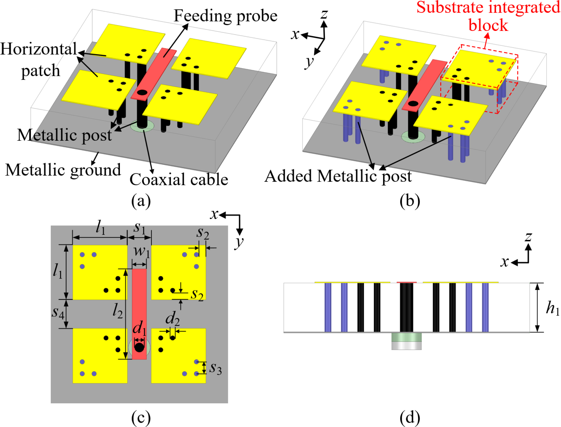
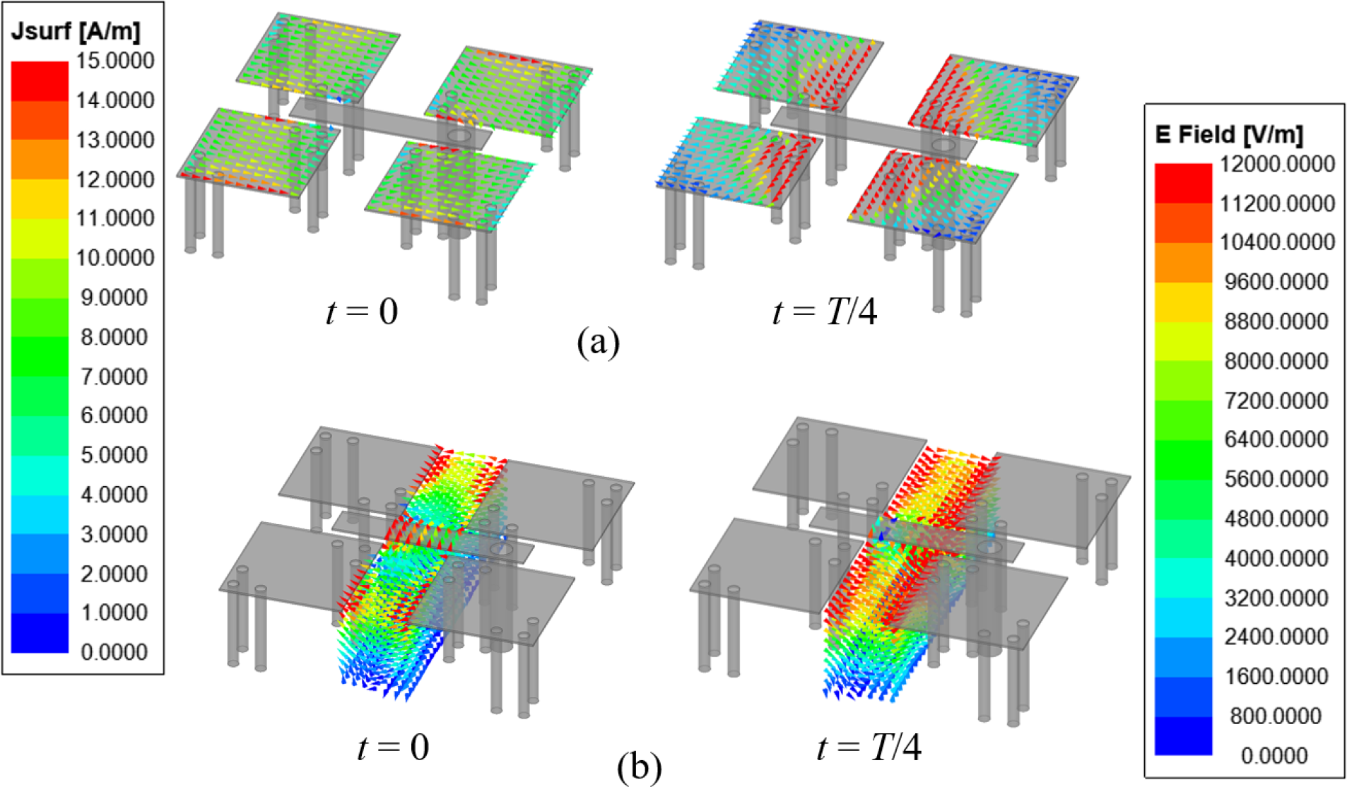
A minor yet crucial modification is then introduced to this conventional design for broadband dual-polarization array application. As shown in Fig. 1(b), by adding additional sets of metallic grounding posts at the opposite diagonal corners of the square patches, four SIBs can, therefore, be realized. The proposed SIBs still offer similar current paths that allow the realizations of both the E- and M-dipoles, as demonstrated by the simulated current distributions and electric fields of the antenna over a quarter periodic of time (T/4) shown in Fig. 2. When t = 0, the current on the horizontal patches reaches its maximum, and the electric fields at the aperture of the gap are weak. When t = T/4, the currents are primarily distributed on the metallic posts near the center that serve as the metallic wall, and the electric fields at the aperture are strong. These simulated field distributions indicate that the proposed ME dipole works properly as expected since the E- and M-dipole are both rightly excited. However, it should be noted that the newly added metallic posts at the four outside corners of the ME dipole would result in the grounding of the patches at the tails, introducing perturbations to not only the E-dipole but also the M-dipole. This would primarily lead to a shift in the operational frequency of the ME dipole. But nearly the same impedance bandwidth compared to the original design can be secured if the geometry is well optimized for good matching.
- electric dipole / magnetic dipole
- 电偶极子是贴片上的水平电流;磁偶极子是接地柱墙与地板缝形成的等效磁流。两者差 T/4 轮流上场,才叫 ME 偶极子。
- L-shaped probe
- L 形探针。竖段从下层穿上来,横段悬在贴片缝里耦合。经典 ME 偶极子的喂法。
- TLY-5
- Taconic 低损耗微波板,εr=2.2。这篇辐射层用 1.575 mm,馈电层后面会换成 0.254 mm。
3. 探针拉开半个周期:双极化不用叠层约 10 分钟
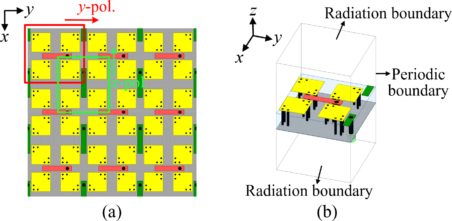
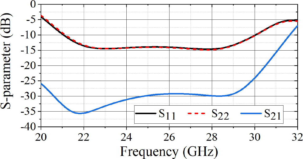
To demonstrate the feasibility of constructing a dual-polarized array using the proposed design, the element is employed to design a two-dimensional array, as shown in Fig. 3(a). By adopting two groups of perpendicularly oriented and interlaced probes, orthogonal linear polarizations can be obtained. In contrast to the conventional dual-polarization feeding approach [13], [14], where the perpendicular probes are placed in close proximity, the probes here are designed to be physically distanced from each other by roughly half of the element spacing, facilitating the implementation of dual-polarization feeding structures and networks in a simpler manner (shown later in Section III). Besides, the introduction of the SIBs makes the radiating structure seen by the two groups of perpendicular probes identical, as indicated by the red and green boxes shown in Fig. 3(a), which leads to similar performances, including the gain and bandwidth for the two polarizations. The corresponding unit cell for fast evaluation of element performance in an array can be found in Fig. 3(b). The simulated S-parameters at the two feeding ports in one unit cell are shown in Fig. 4. The simulated results indicate that the proposed ME dipole achieves an overlapped −10 dB impedance bandwidth of 35.1%, spanning from 21.05 to 30 GHz. The mutual coupling between the two ports is found to be lower than −25 dB in the frequency range of interest.
A conceptual drawing of the proposed dual-polarized array is plotted in Fig. 5(b) and is compared with one typical conventional design [14] shown in Fig. 5(a). In the conventional approach, the crossed-feeding probes are situated at the center of one antenna element, leading to a small probe-to-probe distance and the need of an additional copper layer to avoid direct contact with the two perpendicular probes. In contrast, in the proposed design, the distance between the adjacent perpendicular probes is greatly enlarged. As such, the feeding probes for both polarizations can be designed on the same copper layer, thereby reducing the total substrate layers with a simplified structure. Another notable advantage of this arrangement is that the enlarged distance between orthogonal feeding probes makes the implementation of dual-polarization feeding networks in a single layer more practical.
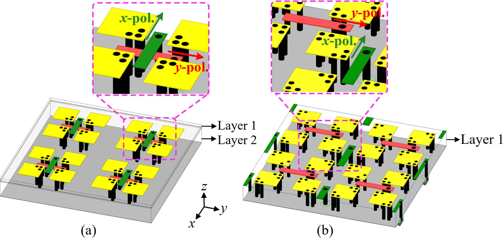
- interlaced probes
- 交错探针。x 极化探针和 y 极化探针不共用一个交叉点,而是在网格里错开约半个周期。
- unit cell / infinite array
- 周期单元。四周 periodic、上下辐射边界,用来快速估阵中单元的匹配和隔离,避免一上来就仿真整阵。
- mutual coupling
- 互耦。这里主要指两路极化端口之间的 S21。无限大阵 < −25 dB,后面实物 < −22.5 dB。
4. 3×3 实物:36.2% 和 14.7 dBi约 10 分钟
As a proof-of-concept validation, a 3 × 3 dual-polarized ME-dipole array is designed, as illustrated in Fig. 6(a). The horizontal portion of the probes and patches are printed on the top side, while the microstrip-line feeding networks are distributed on the bottom surface. An adhesive thin film (Rogers RO4450F) was used to bond the two layers together. By employing nine probes for each polarization to excite the elements, this layout generates a 3 × 3 ME-dipole array for each of the two polarizations. The dimensions of the antenna elements are fine-tuned in the array design to keep a good match. The optimized element spacing is 6.55 mm (0.57λ0) in both of the two directions, where λ0 is the free space wavelength at center frequency f0 (26 GHz). As shown in Fig. 6(b), the microstrip-line feeding network, i.e., the one-to-nine power divider, is designed by cascading several one-to-three equal power dividers. Thanks to the interlaced probe arrangement, two identical feeding networks for launching the two orthogonal polarizations can be realized on the same layer.
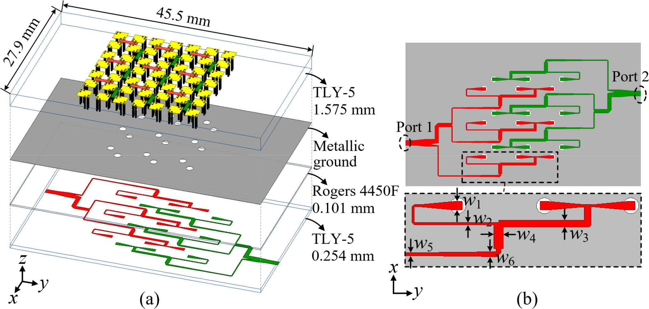
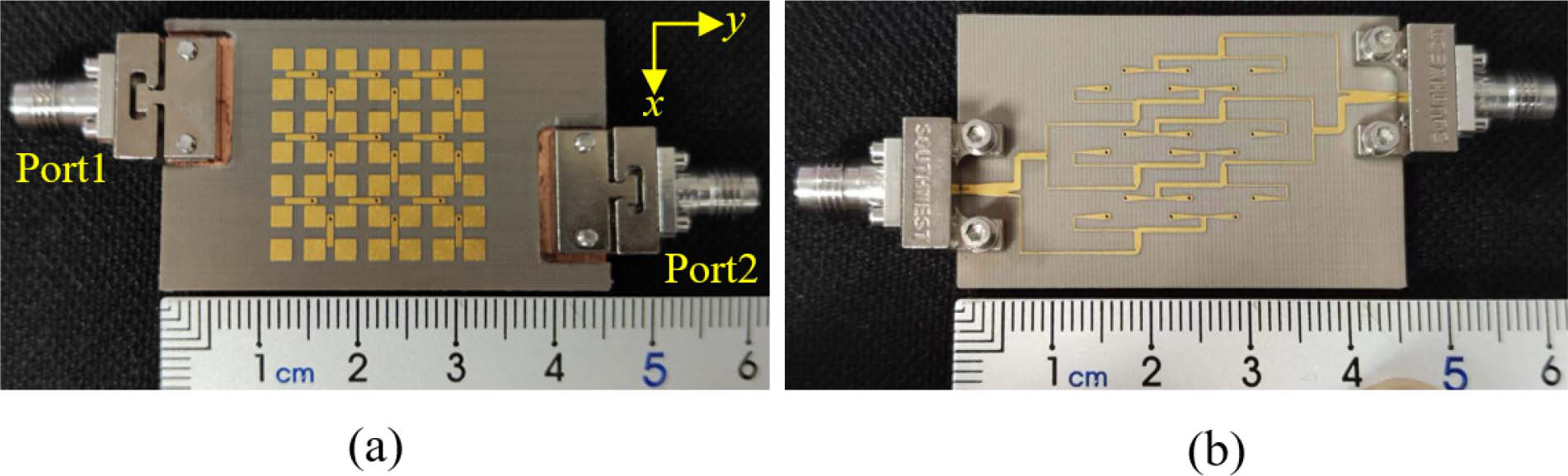
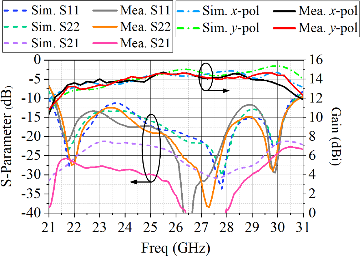
A prototype of the 3 × 3 ME-dipole array, measuring a 46 × 28 mm2 physical size (4 × 2.4λ0²), was fabricated to experimentally validate the methodology. As shown in Fig. 7, a section of the top substrate of the prototype is removed to expose the underlying metallic ground plane by computer numerical control machining for the purpose of realizing better contact of the connectors with the antenna ground plane. A network analyzer was employed to measure the reflection coefficients, while the array performances were characterized in a far-field chamber. S-parameters and gains of the array are depicted in Fig. 8. Good agreement between the simulated and measured S-parameters can be observed. The measured results showcase an overlapped −10 dB bandwidth of 36.2% (from 21.3 to 30.7 GHz), with the |S21| less than −22.5 dB in the same frequency range. The measured gain is up to 14.7 and 14.6 for x- and y-polarizations, respectively. The simulated and measured results show similar trends as frequency changes, though the measured results are slightly lower than the simulated ones from 26 to 31 GHz. The inconsistency is suspected to be caused by fabrication uncertainties. Besides, the variation of gain is within 2 dB in the operational frequency range.
- one-to-nine power divider
- 一分为九。三个一分为三串起来。两路极化各做一套,印在同一层。
- RO4450F
- Rogers 预浸料/粘合膜,这篇用来把辐射层和馈电层粘在一起,厚 0.101 mm。
- gain variation
- 带内增益起伏。摘要和实测都卡在 2 dB,是'方向图稳'的量化说法。
5. 方向图、对照表、该带走什么约 8 分钟
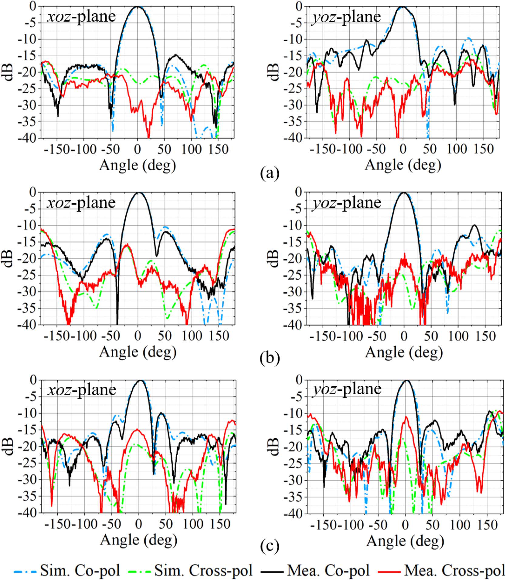
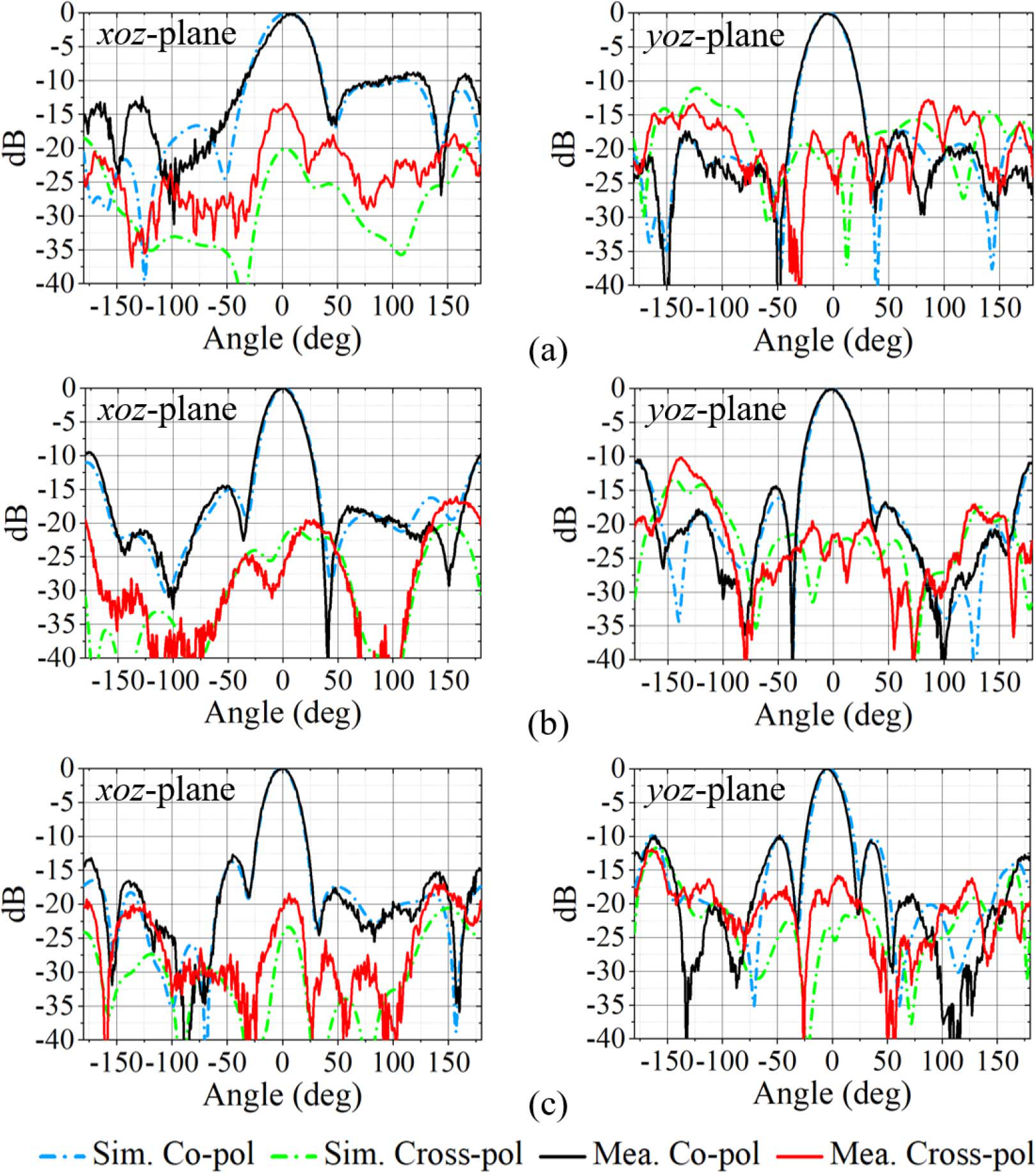
Figs. 9 and 10 illustrate the simulated and measured radiation patterns of the two polarizations at 21.5, 26, and 30.5 GHz. The results agree well with each other in terms of the beamwidth and the sidelobe level. The beamwidth of the main lobe gradually decreases as the frequency increases. The side lobe level remains below −10 dB for both of the two polarizations across the operating band. The cross-polarization at main beam directions is lower than −13 dB at 21.5 and 26 GHz and around −11 dB at 30.5 GHz. In addition, the two polarizations show similar performance, but with slight differences in sidelobe level and cross-polarization. As shown in Fig. 6, the two feeding networks can be regarded as placed along the y-axis, while the two sets of probes are placed along the x- and y-axis, respectively. The discrepancy between the radiation patterns of the two polarizations can be attributed to the difference in the relative positions of their radiating structures and feeding networks.
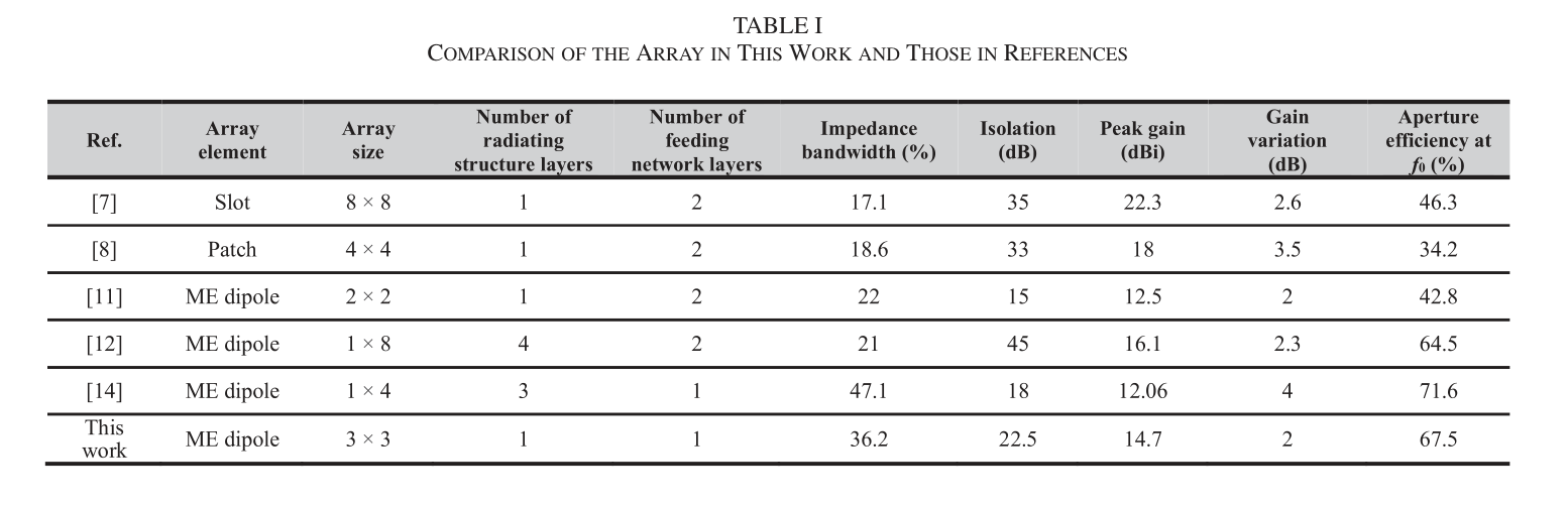
The configurations and performance metrics of previously published dual-polarized antenna array designs are summarized and compared with the proposed work in Table I. Compared with designs reported in [7], [8], [11], and [12], this work shows a wider impedance bandwidth of 36.2%. Benefitting from the SIB-based design approach and interlaced perpendicular feeding probes, the proposed array has less substrate layers than the reported designs, which is cost-effective and easier to fabricate. Moreover, the nearly identical array performances for the two polarizations are also obtained, further balancing the performance of gain stability and bandwidth.
A broadband dual-polarized 3 × 3 ME-dipole antenna array has been proposed in this work for mmW application. By utilizing the SIBs and interlaced perpendicular feeding probes, the array achieves balanced dual-polarization performances within a wide frequency range in a simple structure. The fabricated prototype experimentally demonstrates an overlapped impedance bandwidth of 36.2%, a maximum gain of 14.7 dBi and a gain variation of less than 2 dB. The attractive dual-polarization characteristics, as well as the single-layered radiating structure, make the proposed array competitive for many portable applications.
- aperture efficiency
- 口径效率。Table I 里本文 67.5%(中心频率)。3×3 小阵这个数好看,放大阵还要重新验照射和互耦。
- cross-polarization
- 交叉极化。主瓣方向本文 21.5/26 GHz < −13 dB,30.5 GHz 约 −11 dB,高频是弱项。
- 回到 Obsidian,打开 [[P03-A Broadband Dual-Polarized ME-Dipole Antenna Array for Millimeter-Wave Applications]],用你自己的话写下:
- 1. SIB 相对 Fig. 1(a) 的经典 ME 偶极子,到底改了哪一刀?这刀是为带宽还是为布线?
- 2. 交错探针如何让两路极化看到同一套辐射结构?画一张你自己的红框绿框。
- 3. 若把这个单元拿去当可重构阵的辐射体,0.57λ0 间距和单层馈电,哪个会先成为瓶颈?
- 你在笔记里写过『单元的结构基础』——读完这三问,把那句话展开成自己的判断。